13 kV RMU Fault Detection
Mixed-signal front-end with high-isolation for partial-discharge sensing on live grid assets.
Read case study

Capability
Schematic capture through fab-ready gerbers, by engineers who take the resulting boards through bring-up, EMC pre-compliance and production themselves. Layout choices are made with the whole product in view - the firmware that will run, the enclosure it sits inside, the chamber it will one day be measured in.
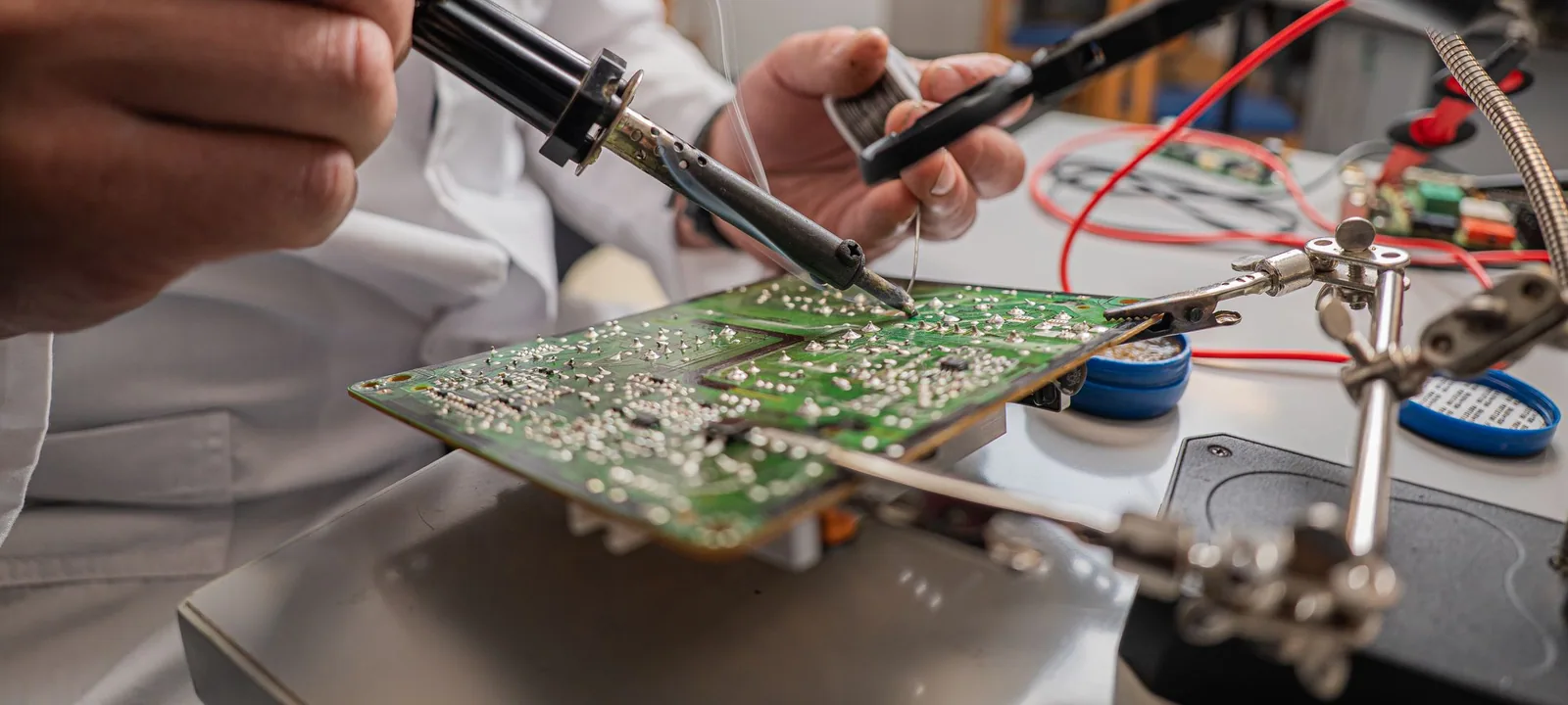
Scope
PCB design is the discipline of turning a set of electrical constraints into a manufacturable board. We treat it as a system problem: the layer stackup, the return-path plan and the placement decisions upstream of routing set the ceiling on EMC, signal integrity and thermal outcomes downstream.
Outcomes
A layout is not a deliverable - a manufacturable, testable board that meets its constraints is. The outcomes that recur across the boards we ship:
DFM review before gerber release catches the pad-size errors, missing fiducials and impossible densities that assemblers charge respin fees to work around. First-pass yield on our prototype runs is measured at the assembly line, not assumed.
Stackup, decoupling and return-path plans decided in week one - not after a failed pre-compliance day. When a design has an emissions problem waiting inside it, we say so in the design review.
Copper pours, cutouts and component placement chosen to hit measured junction temperatures - not simulated ones from optimistic ambient assumptions.
Hierarchical schematics with real net-class rules, documented stackups, and BOM alternates flagged where a single-source part could kill a production run.
Process
Four phases with a real deliverable at each gate - you always know what you paid for and what ships next.
PHASE 01
We start from the constraint that binds - power, latency, thermal, certification - and design backwards from it. You leave with a written architecture, a budget range and the risks named, whether or not we build it.
PHASE 02
Schematics, mechanical and firmware architecture proceed in parallel. High-risk blocks get simulated or breadboarded before the full layout commits.
PHASE 03
Iterative revisions against real bench and field testing. You see every revision, not just the last one. Integration is continuous, not a phase.
PHASE 04
Pilot in the field, closure with the contract manufacturer, production test procedures, and a commissioning-grade handover pack.
Technologies
The platforms we reach for most. If a project needs something not on this list, we say so - the tool is chosen for the constraint, never to fit our habits.
Industries
Deliverables & IP
Every PCB project hands over: schematic source (Altium or KiCad native), PCB source with impedance-controlled stackup documented, complete fabrication package (gerbers, drill, netlist, IPC-2581 or ODB++), assembly package (BOM with distributor part numbers plus alternates, pick-and-place, test-point list), impedance report where applicable, and a design-decision log so a future engineer can read why a choice was made, not just what. All foreground design work transfers to you on payment.
Case studies
Every entry links to the full case study - constraints, what we built, and what it measured afterwards.
Mixed-signal front-end with high-isolation for partial-discharge sensing on live grid assets.
Industrial-carrier board for line-side inference with sub-40 ms deterministic paths.
Multi-input meter interface designed for retrofit into live switchboards.
Compliance
Boards destined for Australian sale carry the RCM; radio products add ACMA obligations; export products layer CE and FCC on top. We design for EMC at the layout stage: proper reference planes, controlled return paths, filtering at every I/O boundary, and shielding budgeted before the enclosure closes around it. Pre-compliance scans against real spectrum analysers happen before formal chamber time is booked.
Safety-critical or high-voltage boards get creepage/clearance rules baked into the schematic capture, not chased at layout. Boards for functional-safety systems get design reviews aligned with the target standard’s expectations. Where the standard demands a certified partner (medical devices, automotive functional safety), we say so up front.
FAQ
Why Incendio
PCB design detached from the firmware, mechanical and chamber-testing that comes next produces boards that pass DRC and fail everywhere else. We hold the whole product view - the firmware that will run, the enclosure it sits inside, the chamber it will be measured in - which is why our first-pass fab yield and first-chamber EMC pass rate are why teams keep coming back.
Related practices: embedded systems development, firmware development, hardware product development, IoT development.
Start
A latency budget, a power budget, a certification date. We reply within one business day - and we’ll say so if we’re not the right team.